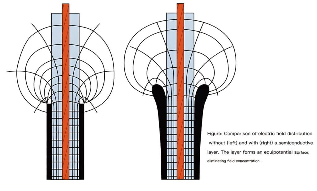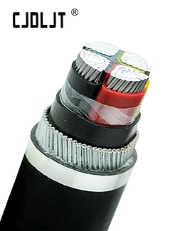
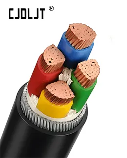
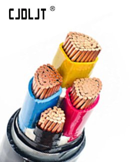
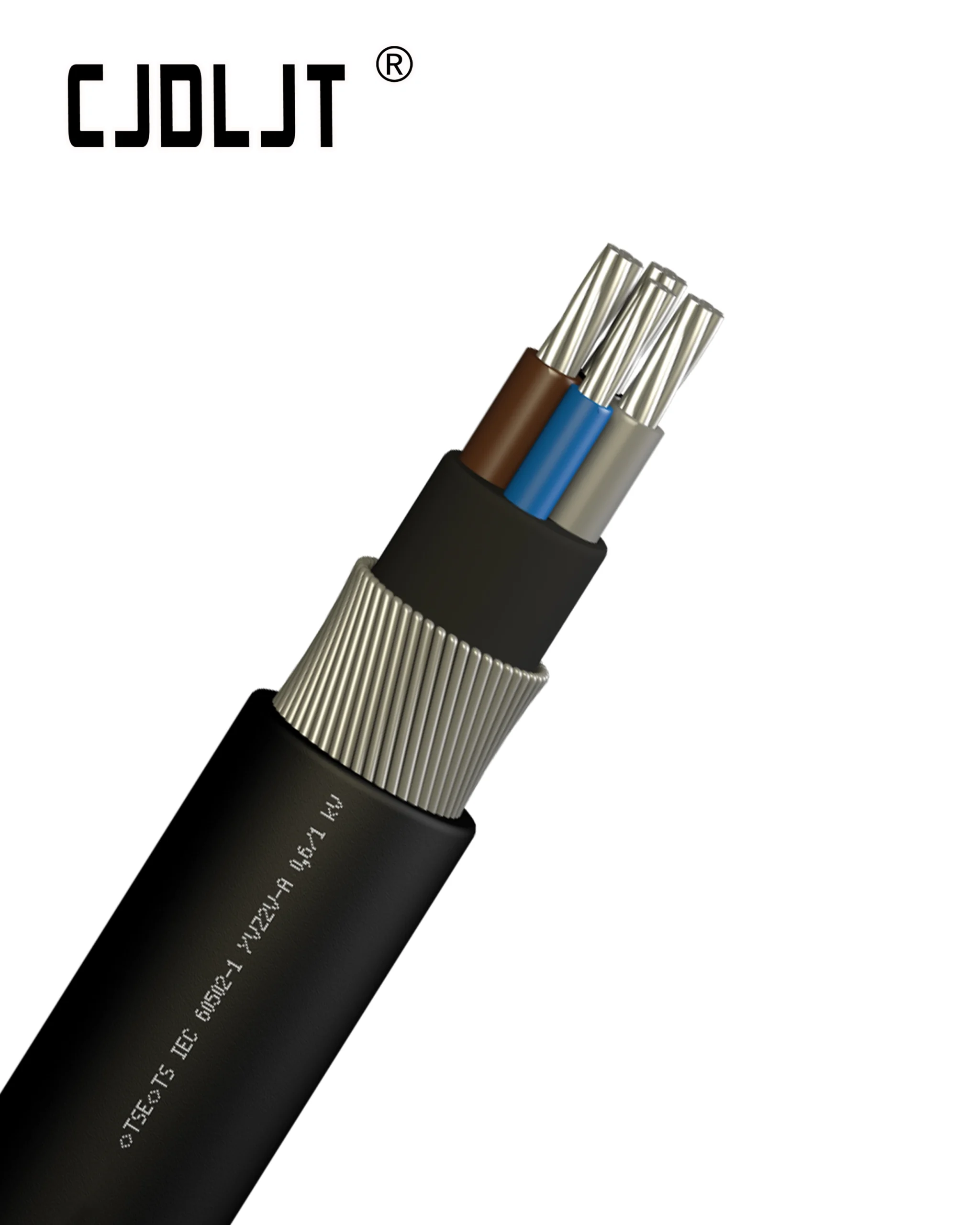


The semi-conductive layer of a cable (also known as the semicon layer or screen) is a critical electrical field-smoothing barrier placed between the metallic components and the primary insulation. In medium- to extra-high-voltage cables, there are two distinct layers applied via a three-layer co-extrusion process: the Conductor Screen (inner semicon) and the Insulation Screen (outer semicon).
Typically made of a polyethylene base heavily compounded with conductive Carbon Black, these layers possess an intermediate electrical resistivity 10¹ ~ 10⁴ Ω·cm. Their core function is to eliminate localized electric field stress concentrations caused by the air gaps and irregularities on stranded conductors or metallic Armor, ensuring a perfectly uniform radial electric field gradient across the Cross-linked Polyethylene (XLPE) dielectric.
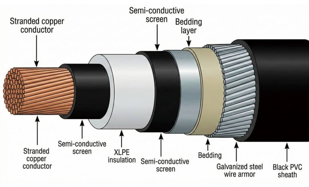
Technical Parameter Matrix: Inner vs. Outer Semi-Conductive Layers
The physical positioning and performance mandates for the two semi-conductive screens defined under standards like IEC 60502-2 are outlined in the data matrix below:
| Technical Parameter | Conductor Screen (Inner Semicon) | Insulation Screen (Outer Semicon) |
| Physical Location | Between the stranded conductor and the XLPE insulation. | Between the XLPE insulation and the metallic shield/copper tape. |
| Primary Electrical Function | Eliminates field concentration from individual wire strands. | Eliminates field concentration from shield wrinkles; maintains ground potential. |
| Material Base | XLPE/CPE filled with high-purity Carbon Black | Strippable or fully bonded semi-conductive compound |
| Volume Resistivity at 20°C | ≤ 500 Ω・cm (Standard limit) | ≤ 500 Ω・cm (Standard limit) |
| Volume Resistivity at 90°C | ≤ 1000 Ω·cm (Elevated state) | ≤ 1000 Ω・cm (Elevated state) |
| Interface Smoothness Target | Microscopic protrusions < 15 | Microscopic protrusions < 15 μm |
Engineering Physics: Why the Semi-Conductive Layer is Indispensable
Faraday Cage Effect and Boundary Smoothing
If a high-voltage stranded conductor were directly surrounded by a raw dielectric like XLPE, the helical geometric profile of the individual outer wire strands would create severe distortions in the electric field lines. The air gaps trapped in the valleys between the strands would experience massive localized voltage gradients due to the permittivity mismatch (εᵣ = 1 for air vs. εᵣ = 2.3 for XLPE). This would cause the air to ionize instantly, launching localized Partial Discharge and destructive Electrical Treeing.
By placing the inner semi-conductive layer directly over the strands, the material penetrates the valleys and encapsulates the conductor. Because it conducts electricity (albeit with high resistance relative to copper), the outer boundary of this layer becomes an equipotential surface. It acts exactly like a microscopic Faraday Cage, smoothing out the radial electric field lines into a perfectly concentric, uniform pattern, as defined by Gauss’s Law for coaxial configurations:
E = V / (r · ln(Ro / Ri))
Where the effective inner radius (Rᵢ) is smoothly extended to the outer perimeter of the inner semi-conductive screen, eliminating any sharp geometrical field variations.